


Chinese researchers have announced a groundbreaking advancement in semiconductor manufacturing, revealing a new technique that can reduce microchip defects by as much as 99%. This development promises to enhance the quality of domestic microchip production, a critical area for China’s technological independence.
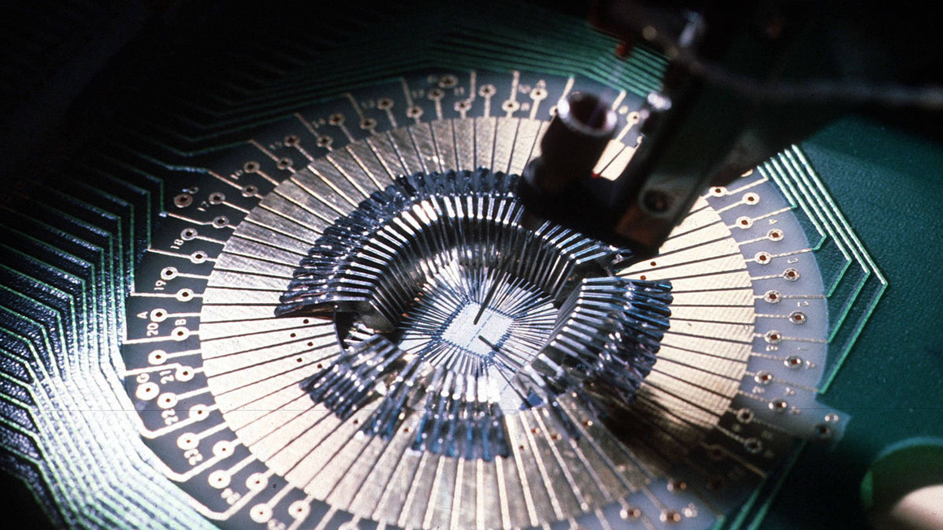
The innovation stems from a collaborative effort involving Professor Peng Hailin and teams from Peking University, Tsinghua University, and the University of Hong Kong (HKU). Their research focuses on improving the photolithography process, a crucial step in producing computer chips. This technique involves using light to create intricate circuit patterns on silicon wafers, akin to developing a microscopic photograph.
During photolithography, a light-sensitive liquid known as photoresist is applied to silicon wafers. Ultraviolet light is then projected through a patterned mask to develop the circuit design. While effective, this process can lead to significant manufacturing issues. For instance, during the development phase, some of the dissolved photoresist can form tiny clumps that stick to the wafer, causing defects that can compromise the functionality of chips.
At nanometer scales, even a particle measuring just 30 nanometers can render a chip unusable, resulting in substantial financial losses. Until now, the dynamics within the developer liquid remained largely unobservable, complicating manufacturers’ efforts to troubleshoot these defects.
To address this challenge, the research team employed a technique known as cryo-electron tomography (cryo-ET). Traditionally used in biology for detailed cellular studies, cryo-ET allows researchers to freeze the development process at 32°F (–175°C), capturing a snapshot of the chemical interactions in real time.
By utilizing this approach, the team was able to visualize the behavior of photoresist molecules during development. They discovered that these molecules tend to tangle together, forming particles as large as 30–40 nanometers. Crucially, they found that approximately 70% of the photoresist molecules do not dissolve properly; instead, they linger at the air-liquid interface, only to redeposit on the wafer during rinsing, thus causing defects.
With these insights, the researchers proposed two straightforward yet impactful modifications to existing chip fabrication techniques. The first involves slightly increasing the bake temperature after exposure to minimize polymer tangles. Their tests indicated that this adjustment significantly reduces the formation of clumps.
The second modification improves the rinse process by altering the fluid flow to effectively sweep away problematic polymers before they can reattach to the wafer surface. When applied to 12-inch (30.5 cm) wafers, these changes led to a remarkable reduction in defect counts, achieving near-perfect lithography quality.
This innovation not only enhances the efficiency of semiconductor manufacturing but also transforms a previously opaque and complex process into one that is clearer and more controllable. The research marks a significant milestone for China’s semiconductor industry, as it strives for greater self-sufficiency and technological advancement in an increasingly competitive global landscape.
As Professor Peng Hailin noted, “By freezing and visualizing what happens in the developer, we can turn a long-unsolved problem into one that can be understood and controlled.” This breakthrough stands to reshape the future of microchip production, potentially setting new standards in the industry.