


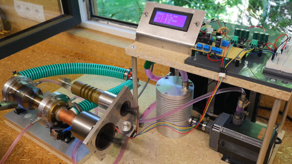


A team from Columbia University has achieved a significant advancement in optical technology by developing a method to enhance nonlinear optical effects at the nanoscale. Led by Jim Schuck, a professor of mechanical engineering, the researchers created a crystalline device only 3.4 micrometers thick capable of generating entangled photon pairs, which are vital for the evolving field of quantum technologies.
This groundbreaking work was detailed in a paper published in Nature Photonics in October 2025. The Columbia team successfully reduced the size of nonlinear optical platforms to just 160 nanometers by employing metasurfaces—artificial structures etched into ultrathin crystals that grant them new optical properties. According to Chiara Trovatello, the corresponding author and currently an assistant professor at Politecnico di Milano, “We’ve established a successful recipe to pattern ultrathin crystals at the nanoscale to enhance nonlinearity while maintaining their sub-wavelength thickness.”
Innovative Techniques for Quantum Applications
The Schuck lab focuses on transition metal dichalcogenides (TMDs), a class of crystals that can be thinned down to atom-thin layers. These layers, while exhibiting high nonlinearity, have struggled to efficiently generate photons at new frequencies compared to traditional nonlinear crystals found in everyday devices like laser pointers. Trovatello explained, “Size doesn’t matter for something like a laser pointer. But for quantum technologies, like quantum processors, size becomes crucial.”
Currently, the leading sources of qubits occupy considerable space, often filling entire rooms, reminiscent of early classical computers. To facilitate the scalability of quantum technologies, the team aims to miniaturize qubit sources. Their previous research, published in January 2025, utilized a technique known as periodic poling to optimize the optical output of molybdenum disulfide by layering it in alternating directions. This method ensured that the light waves were phase-matched and did not interfere with each other.
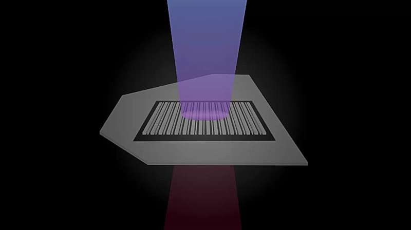
In their recent work, the researchers introduced a complementary platform featuring TMDs with customizable etched metasurfaces. The metasurface technology allows the introduction of optical properties that do not exist in unmodified crystals. By selectively removing sections of atoms, the team can create new periodic geometries that enhance optical effects.
A Simple Yet Effective Method
Ph.D. student and first author Zhi Hao Peng developed the nanofabrication technique used to etch repeating lines onto molybdenum disulfide. “Our design enhances the nonlinear effects much more than traditional linear optical optimization techniques, achieving strong enhancement not previously possible,” Peng stated. Their metasurface technology improved second-harmonic generation—where two photons combine into one—with an enhancement of nearly 150 times compared to unpatterned samples.
As the researchers optimize this process, their next goal is to reverse it, splitting a single photon into two entangled photons. Notably, Peng’s approach simplifies the fabrication process, making it more cost-effective and efficient than previous methods. Schuck noted, “Nonlinear crystals have been vital in many photonic technologies, but they can be brittle and challenging to shape. Peng developed a deceptively simple technique that allows for increasingly complex patterns using standard cleanroom etching technologies.”
Theoretical collaborators, including Andrea Alu from the CUNY Advanced Science Research Center, assisted in determining the necessary metasurface patterns to enhance TMDs’ nonlinear response. Alu remarked, “This work demonstrates how engineered nonlocalities in metasurfaces can unlock unprecedented nonlinear efficiencies when combined with 2D materials.”
The combination of metasurfaces with 2D crystals marks a significant step in photonics, potentially leading to compact and integrable platforms for nonlinear optics. The light produced operates at telecommunications-range wavelengths, making it compatible with existing networks and devices. Schuck concluded, “This could be one of the most compact sources of entangled photons at that wavelength range. With our footprint, we can really start to think about fully on-chip quantum photonics.”
Further information can be found in the publication by Zhi Hao Peng et al titled “3R-stacked transition metal dichalcogenide non-local metasurface for efficient second-harmonic generation” in Nature Photonics (2025).