


A team of researchers has made significant strides in improving the brightness and image clarity of augmented reality (AR) glasses through the development of a new optical component. This advancement could bring AR glasses closer to widespread adoption, akin to today’s smartphones.
Leading the research, Nick Vamivakas from the University of Rochester highlighted the current limitations of many AR headsets, which often come with bulky designs, short battery life, and displays that struggle to perform in bright outdoor conditions. “By creating a much more efficient input port for the display, our work could help make AR glasses much brighter and more power-efficient,” he stated. The goal is to transition AR glasses from niche products to lightweight and comfortable accessories.
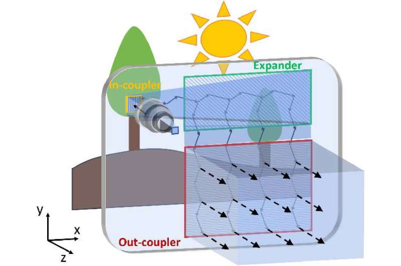
The findings were published in the journal Optical Materials Express on November 11, 2025. The researchers innovated by replacing the conventional single waveguide in-coupler—the component that channels images from a micro-display into the lenses—with a new design incorporating three specialized zones made from metasurface material. This design aims to enhance performance markedly.
“Our work provides the first experimental proof that this complex, multi-zone design works in the real world,” Vamivakas explained. While the focus is on AR applications, the technology has potential uses in various compact optical systems, including head-up displays for automotive or aerospace sectors and advanced optical sensors.
Metasurfaces are ultra-thin materials with features smaller than a human hair, which allow for bending, focusing, or filtering light in ways that traditional optics cannot achieve. “They offer greater design and manufacturing flexibility than conventional optics,” Vamivakas noted, underscoring the broader implications of this technology for optical system design.
To create the innovative in-coupler, the team developed metasurface patterns that efficiently capture incoming light and minimize light leakage. This design also preserves the shape of incoming light, which is crucial for maintaining high image quality. The research builds upon earlier theoretical work indicating that a multi-zone in-coupler would yield optimal efficiency and image quality.
Advancements in metasurface gratings have provided the necessary design flexibility, while cutting-edge fabrication techniques, including electron-beam lithography and atomic layer deposition, enabled the precise construction of complex nanostructures. “This paper bridges the gap from idealized theory to practical, real-world application,” Vamivakas emphasized.
The researchers conducted a series of tests to validate the new in-coupler. They fabricated and evaluated each of the three metasurface zones individually and then assembled the complete three-zone device. Testing revealed a total coupling efficiency across the horizontal field of view from -10° to 10°. The average measured efficiency was 30%, closely aligning with the simulated average of 31%. The only notable discrepancy occurred at the edge of the field of view at -10°, where measured efficiency was 17% compared to a simulated 25.3%. This was attributed to the design’s heightened angular sensitivity at that point.
Looking ahead, the research team is working to apply this metasurface design to other components of the waveguide system. Their goal is to develop a complete, high-efficiency metasurface-based system. Plans also include expanding the design from single-color (green) operation to full RGB functionality, while refining the design to improve fabrication tolerance and reduce efficiency drops at the edges of the field of view.
For practical commercialization of this technology, a fully integrated prototype is essential, pairing the in-coupler with a real micro-display engine and an out-coupler. Additionally, the development of a robust, high-throughput manufacturing process will be necessary to replicate the intricate nanostructures cost-effectively.
Further details can be found in the research article titled “Design and experimental validation of a high-efficiency multi-zone metasurface waveguide in-coupler,” authored by Pei Xiong and colleagues, published in Optical Materials Express.